IntelliGenes accessible AI software helps predict diseases

To help predict diseases, researchers at Rutgers Health have developed IntelliGenes software, which combines artificial intelligence (AI) and machine-learning approaches.

A study published in Bioinformatics explains how IntelliGenes can be used by a wide range of users to analyze multigenomic and clinical data. It’s accessible by anyone, says Zeeshan Ahmed, lead author of the study and a faculty member at Rutgers Institute for Health, Health Care Policy and Aging Research (IFH).

Personalized patient predictions

Previously, there were no AI or machine-learning tools available to investigate and interpret the complete human genome, especially for non-experts. So Ahmed and members of his Rutgers lab developed IntelliGenes software. It combines conventional statistical methods with cutting-edge machine-learning algorithms to produce personalized patient predictions and a visual representation of the biomarkers significant to disease prediction.

In another study, published in Scientific Reports, the researchers applied IntelliGenes to discover novel biomarkers and predict cardiovascular disease with high accuracy.

“There is huge potential in the convergence of datasets and the staggering developments in artificial intelligence and machine learning,” said Ahmed, who is also an assistant professor of medicine at Robert Wood Johnson Medical School.

Early detection of common and rare diseases

IntelliGenes can support personalized early detection of common and rare diseases in individuals, as well as open avenues for broader research ultimately leading to new interventions and treatments,” said Ahmed.

The researchers tested the software using Amarel, a high-performance computing cluster managed by the Rutgers Office of Advanced Research Computing.

Citation: DeGroat, W., Mendhe, D., Bhusari, A., Abdelhalim, H., Zeeshan, S., & Ahmed, Z. (2023). IntelliGenes: A novel machine learning pipeline for biomarker discovery and predictive analysis using multi-genomic profiles. Bioinformatics, 39(12). https://doi.org/10.1093/bioinformatics/btad755

Citation: DeGroat, W., Abdelhalim, H., Patel, K. et al. Discovering biomarkers associated and predicting cardiovascular disease with high accuracy using a novel nexus of machine learning techniques for precision medicine. Sci Rep 14, 1 (2024). https://doi.org/10.1038/s41598-023-50600-8

Let us know your thoughts! Sign up for a Mindplex account now, join our Telegram, or follow us on Twitter

Robotics At The Nanoscale: A DNA-Based Electromotor Powered by Nanopore Flow

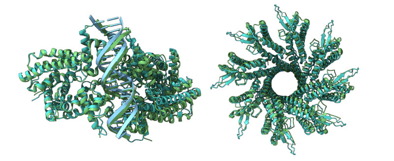
Scientists have created the world’s first working nanoscale electromotor. Using a turbine engineered from DNA, it’s powered by hydrodynamic flow inside a nanopore (a nanometer-sized hole in a membrane) of solid-state silicon nitride, according to a paper published in the journal Nature Nanotechnology.

The researchers say the electromotor could help spark research in future applications, such as building molecular factories to create useful chemicals or medical probes based on molecules inside the bloodstream to detect diseases.

Designing at the nanoscale

DNA turbine powered by a transmembrane potential across a nanopore (credit: X. Shi et al.)

“Common macroscopic machines become inefficient at the nanoscale,” said study co-author professor Aleksei Aksimentiev, a professor of physics at the University of Illinois at Urbana-Champagne. “We have to develop new principles and physical mechanisms to realize electromotors at the very, very small scales.” 

That work was headed by Hendrik Dietz of the Technical University of Munich and Cees Dekker of the Delft University of Technology.

Dietz, a world expert in DNA origami, manipulated DNA molecules to make the tiny motor’s turbine, consisting of 30 double-stranded DNA helices. Decker’s lab work demonstrated how the turbine rotates by applying an electric field.

Aksimentiev’s lab carried out all-atom molecular dynamics simulations on a system of five million atoms to characterize the physical phenomena of how the motor works, using the National Science Foundation (NSF)-funded Frontera, the top academic supercomputer in the U.S. Aksimentiev also had access to the NSF-funded Advanced Cyberinfrastructure Coordination Ecosystem: Services & Support (ACCESS) and to Expanse of the San Diego Supercomputer Center and Anvil of Purdue University.

DNA as an electromotor

The DNA nanoturbine, which can rotate up to a billion revolutions per minute, builds on a previous study that showed that a single DNA helix is the tiniest electromotor that one can build. DNA has emerged as a building material at the nanoscale, according to Aksimentiev. “This new work is the first nanoscale motor where we can control the rotational speed and direction,” he said.

“In the future, we might be able to synthetize a molecule using the new nanoscale electromotor, or we can could use it to as an element of a bigger molecular factory, where things are moved around, he added. “Or we could imagine it as a vehicle for soft propulsion, where synthetic systems can go into a bloodstream and probe molecules or cells, one at a time.”

In the movie Fantastic Voyage, a team of Americans in a nuclear submarine is shrunk and injected into a scientist’s body to quickly fix a blood clot. Aksimentiev said something like this could actually happen (except for the miniature people part).

Citation: Shi, X., Pumm, AK., Maffeo, C. et al. A DNA turbine powered by a transmembrane potential across a nanopore. Nat. Nanotechnol. (2023). https://doi.org/10.1038/s41565-023-01527-8 (open-access)

Let us know your thoughts! Sign up for a Mindplex account now, join our Telegram, or follow us on Twitter

‘Magic trap’ preserves quantum coherence in ultracold molecules longer than expected

In recent research, Rice University and Durham University scientists were able to prolong quantum behavior in an experimental system nearly 30-fold by using ultracold temperatures and laser wavelengths. These generated a “magic trap” that helped delay the onset of decoherence.

Generally, the coherence of this rotating behavior in ultracold molecules decays over a very short amount of time, note the researchers. Before now, the longest recorded quantum state of rotating molecules was 1/20th of a second.

A magic wavelength of light

The researchers were inspired by theoretical work by Temple University’s Svetlana Kotochigova that suggested a certain “magic” wavelength of light could preserve quantum coherence for a longer period of time.

The Rice Hazzard Group applied this theory in the laboratory in a new experimental technique. They created a “magic trap” that kept the molecules rotating quantum mechanically for nearly 1.5 seconds ⎯ a 30-fold increase.

The study, published in Nature Physics, is the first experimental demonstration of its kind and provides a new arena to study quantum interactions, the researchers say.

The research was supported by the U.K. Engineering and Physical Sciences Research Council, U.K. Research and Innovation Frontier Research, the Royal Society, Durham University, the Robert A. Welch Foundation, the National Science Foundation, the Office of Naval Research, the W.F. Keck Foundation and the U.S. Air Force Office of Scientific Research.

Citation: Gregory, P.D., Fernley, L.M., Tao, A.L. et al. Second-scale rotational coherence and dipolar interactions in a gas of ultracold polar molecules. Nat. Phys. (2024). https://www.nature.com/articles/s41567-023-02328-5 (open-access)

Let us know your thoughts! Sign up for a Mindplex account now, join our Telegram, or follow us on Twitter

Next (Little) Thing: Insect-like Mini-robots

Engineers at Washington State University have developed two miniature bug-like robots that could be used in the future for work in areas such as artificial pollination, search and rescue, insect control, environmental monitoring, micro-fabrication and robotic-assisted surgery. (Also great for creepy-crawler pranks?)

The two mini-bugs weigh in at just 8 milligrams and 55 milligrams, and can move at about six millimeters a second—way slower than ants, who can run at a meter/sec.

How they work

The trick: tiny actuators make the robots move, weighing less than a milligram—the smallest known to have been developed for micro-robotics, said Néstor O. Pérez-Arancibia, Flaherty Associate Professor in Engineering at WSU’s School of Mechanical and Materials Engineering, who led the project. 

The actuator uses a material called a “shape memory alloy” (SMA) that is 1/1000th of an inch in diameter and can change shapes and move when heated—no moving parts or spinning components. The SMA technology also requires only a very small amount of electricity or heat to make them move.

Water strider next

The researchers would next like to copy another insect and develop a water strider-type robot that can move across the top of the water surface as well as just under it.

They are also working to use tiny batteries or catalytic combustion to make their robots fully autonomous and untethered from a power supply.

Citation: C. K. Trygstad, X. -T. Nguyen and N. O. Pérez-Arancibia, “A New 1-mg Fast Unimorph SMA-Based Actuator for Microrobotics,” 2023 IEEE/RSJ International Conference on Intelligent Robots and Systems (IROS), Detroit, MI, USA, 2023, pp. 2693-2700, doi: 10.1109/IROS55552.2023.10342518.

Let us know your thoughts! Sign up for a Mindplex account now, join our Telegram, or follow us on Twitter

New Sensors Record One Or Two Neurons Deep In The Brain

New sensors are capable of recording activity deep within the brain from large populations of individual neurons, with a resolution of as few as one or two neurons, according to a study published in the Jan. 17, 2024 issue of the journal Nature Communications.

The research team is led by the Integrated Electronics and Biointerfaces Laboratory (IEBL) at the University of California San Diego.

High-resolution sensing

The new approach relies on ultra-thin, flexible and customizable probes made of clinical-grade materials and equipped with sensors that can record extremely localized brain signals. The probes are much smaller than today’s clinical sensors, so they can be placed extremely close to one another, allowing for high-resolution sensing in specific areas at unprecedented depths within the brain. 

The probes can record with up to 128 channels (the state of the art in today’s clinical probes is only 8 to 16 channels). The researchers plan to develop future versions that can expand the number of channels to thousands per probe, dramatically enhancing physicians’ ability to acquire, analyze and understand brain signals at a higher resolution. 

Wireless monitoring of epilepsy patients up to 30 days

This technology, called “UC San Diego Micro-stereo-electro-encephalography (µSEEG),” is a first step towards precision wireless monitoring of patients with treatment-resistant epilepsy for extended periods of time—up to 30 days—as they go about their daily lives. Other potential applications include helping people with Parkinson’s disease, movement disorders, obsessive-compulsive disorder, obesity, treatment-resistant depression, high-impact chronic pain and other disorders.

The new probes can also provide therapeutic electrical stimulation to precise locations on the surface of the brain cortex. They are 15 microns thic (about 1/5th the thickness of a human hair) and are extremely compact, minimizing the differences between the material properties of the probe and the brain.

These sensors will communicate wirelessly with a small computer system in a wireless cap, which a person could wear for extended periods of time. This cap would provide wireless power and the computational infrastructure to capture the brain signals being recorded from a person’s brain for 30 days

Experimental subjects

In the new paper, the team reports the functioning of the new system in two human patients. The team also presents data from a series of different animal models, including successful recordings from rat barrel cortex in both acute and chronic settings; recording of the somatosensory cortex in an anesthetized pig; and recordings in non-human primates at different depths inside the brain. 

Citation: Lee, K., Paulk, A.C., Ro, Y.G. et al. Flexible, scalable, high channel count stereo-electrode for recording in the human brain. Nat Commun 15, 218 (2024). https://doi.org/10.1038/s41467-023-43727-9 (open-access)

Let us know your thoughts! Sign up for a Mindplex account now, join our Telegram, or follow us on Twitter

Caltech space solar power project ends first in-space mission with successes and lessons

Last June, Caltech’s Space Solar Power Demonstrator (SSPD-1) launched into space to demonstrate and test three technological innovations needed to make space solar power a reality, as we reported in Mindplex News.

Now, with SSPD-1’s mission in space concluded, engineers on Earth are celebrating the testbed’s successes and learning important lessons that will help chart the future of space solar power. All of the experiments aboard SSPD-1 were ultimately successful.

“Solar power beamed from space at commercial rates (‘lighting the globe’), is still a future prospect. But this critical mission demonstrated that it should be an achievable future,” says Caltech President Thomas F. Rosenbaum, the Sonja and William Davidow Presidential Chair and professor of physics. 

SSPD-1 represents a major milestone in a project that has been underway for more than a decade, consisting of three main experiments, each testing a different technology are ultra-lightweight, cheap, flexible, and deployable:

  • DOLCE (Deployable on-Orbit ultraLight Composite Experiment) will eventually become a kilometer-scale constellation to serve as a power station. It had two problems, which were fixed.
  • ALBA: photovoltaic (PV) cells to enable an assessment of the types of cells that can withstand punishing space environments. They tested various designs.
  • MAPLE (Microwave Array for Power-transfer Low-orbit Experiment): an array of flexible, lightweight microwave-power transmitters to demonstrate wireless power transmission at distance in space. MAPLE demonstrated its ability to transmit power wirelessly in space and to direct a beam to Earth—a first in the field. “These observations have already led to revisions in the design of various elements of MAPLE to maximize its performance over extended periods of time,” says Hajimiri, Bren Professor of Electrical Engineering and Medical Engineering and co-director of SSPP.

SSPD-1 will remain in orbit to support continued testing and demonstration of the vehicle’s Microwave Electrothermal Thruster engines. It will ultimately deorbit and disintegrate in Earth’s atmosphere. Meanwhile, the SSPP team continues work in the lab, studying the feedback from SSPD-1 to identify the next set of fundamental research challenges for the project to tackle.  

Let us know your thoughts! Sign up for a Mindplex account now, join our Telegram, or follow us on Twitter

Machine learning + automated experiments accelerate drug-design process

Researchers from the University of Cambridge have developed a platform that combines automated experiments with AI to predict how chemicals will react with one another, and could accelerate the design process for new drugs.

Predicting how molecules forr the discovery and manufacture of new pharmaceuticals has been a trial-and-error expensive and process, and the reactions often fail.

Reactome

Now the researchers have developed a data-driven “reactome” approach, inspired by genomics, where automated experiments are combined with machine learning to understand chemical reactivity, greatly speeding up the process.

Their results, reported in the journal Nature Chemistry, are the product of a collaboration between Cambridge and Pfizer.

“The reactome could change the way we think about organic chemistry,” said Dr Emma King-Smith from Cambridge’s Cavendish Laboratory, the paper’s first author. The reactome approach picks out relevant correlations between reactants, reagents, and performance of the reaction from the data, and points out gaps in the data itself. The data is generated from very fast, or high throughput, automated experiments.

Machine learning for faster drug design

In a related paper, published in Nature Communications, the team developed a machine learning approach that enables chemists to introduce precise transformations to pre-specified regions of a molecule, enabling faster drug design.

The approach allows chemists to tweak complex molecules—like a last-minute design change—without having to make them from scratch.

Citation: King-Smith, E., Berritt, S., Bernier, L. et al. Probing the chemical ‘reactome’ with high-throughput experimentation data. Nat. Chem. (2024). https://doi.org/10.1038/s41557-023-01393-w

Citation: King-Smith, E., Faber, F.A., Reilly, U. et al. Predictive Minisci late stage functionalization with transfer learning. Nat Commun 15, 426 (2024). 10.1038/s41467-023-42145-1 (open-access)

Let us know your thoughts! Sign up for a Mindplex account now, join our Telegram, or follow us on Twitter

Catalytic combo converts greenhouse gas CO2 to solid carbon nanofibers

Scientists at the U.S. Department of Energy’s (DOE) Brookhaven National Laboratory and Columbia University have developed a way to convert carbon dioxide (CO2), a potent greenhouse gas, into carbon nanofibers.

The new method, which uses tandem electrochemical and thermochemical reactions, runs at relatively low temperatures and ambient pressure.

Locking carbon away

As the scientists describe in the journal Nature Catalysis, this approach could successfully lock carbon away in a useful solid form to offset or even achieve negative carbon emissions.

Unlike current methods, “you can put the carbon nanofibers into cement to strengthen the cement,” said Jingguang Chen, a professor of chemical engineering at Columbia with a joint appointment at Brookhaven Lab who led the research. “That would lock the carbon away in concrete for at least 50 years, potentially longer. By then, the world should be shifted to primarily renewable energy sources that don’t emit carbon.”

As a bonus, the process also produces hydrogen gas (H2), a promising alternative fuel that, when used, creates zero emissions.

The tandem two-step 

“We found a process that can occur at about a relatively low 400 degrees Celsius, which is a much more practical, industrially achievable temperature.”

The trick was to break the reaction into stages and to use two different types of catalysts—materials that make it easier for molecules to come together and react.

The scientists started by realizing that carbon monoxide (CO) is a much better starting material than CO2 for making carbon nanofibers (CNF). Then they backtracked to find the most efficient way to generate CO from CO2.

For the second step, the scientists turned to a heat-activated thermocatalyst made of an iron-cobalt alloy. It operates at temperatures around 400 degrees Celsius, significantly milder than a direct CO2-to-CNF conversion would require. They also discovered that adding a bit of extra metallic cobalt greatly enhances the formation of the carbon nanofibers.

Truly carbon-negative

“By coupling electrocatalysis and thermocatalysis, we are using this tandem process to achieve things that cannot be achieved by either process alone,” Chen said.

If these processes are driven by renewable energy, the results would be truly carbon-negative, opening new opportunities for CO2 mitigation, the researchers say.

Citation: Xie, Z., Huang, E., Garg, S. et al. CO2 fixation into carbon nanofibres using electrochemical–thermochemical tandem catalysis. Nat Catal (2024). https://doi.org/10.1038/s41929-023-01085

Let us know your thoughts! Sign up for a Mindplex account now, join our Telegram, or follow us on Twitter

How to get more out of Moore’s Law and advance electronics

Moore’s Law, a fundamental scaling principle for electronic devices, forecasts that the number of transistors on a chip will double every two years, ensuring more computing power—but a limit exists.

Today’s most advanced chips house nearly 50 billion transistors within a space no larger than your thumbnail. The task of cramming even more transistors into that confined area has become more and more difficult, according to Penn State researchers.

3D integration

In a study published Jan. 10 in the journal Nature, Saptarshi Das, an associate professor of engineering science and mechanics and co-corresponding author of the study, and his team suggest a remedy: seamlessly implementing 3D integration with 2D materials.

In the semiconductor world, 3D integration means vertically stacking multiple layers of semiconductor devices. This approach facilitates the packing of more silicon-based transistors onto a computer chip, commonly referred to as “More Moore,” but also permits the use of transistors made from 2D materials to incorporate diverse functionalities within various layers of the stack, a concept known as “More than Moore.”

With the work outlined in the study, Saptarshi and the team demonstrate feasible paths beyond scaling current tech to achieve both More Moore and More than Moore through monolithic 3D integration. Monolithic 3D integration is a fabrication process wherein researchers directly make the devices on the one below, as compared to the traditional process of stacking independently fabricated layers.

Highest density

“Monolithic 3D integration offers the highest density of vertical connections as it does not rely on bonding of two pre-patterned chips — which would require microbumps where two chips are bonded together — so you have more space to make connections,” said Najam Sakib, graduate research assistant in engineering science and mechanics and co-author of the study.

Monolithic 3D integration faces significant challenges, though, according to Darsith Jayachandran, graduate research assistant in engineering science and mechanics and co-corresponding author of the study, since conventional silicon components would melt under the processing temperatures.

“One challenge is the process temperature ceiling of 450 degrees Celsius (C) for back-end integration for silicon-based chips — our monolithic 3D integration approach drops that temperate significantly to less than 200 C,” Jayachandran said, explaining that the process temperature ceiling is the maximum temperature allowed before damaging the prefabricated structures. “Incompatible process temperature budgets make monolithic 3D integration challenging with silicon chips, but 2D materials can withstand temperatures needed for the process.”

The researchers used existing techniques for their approach, but they are the first to successfully achieve monolithic 3D integration at this scale using 2D transistors made with 2D semiconductors called transition metal dichalcogenides.

Energy-efficient vertical stacking

The ability to vertically stack the devices in 3D integration also enabled more energy-efficient computing because it solved a surprising problem for such tiny things as transistors on a computer chip: distance.

“By stacking devices vertically on top of each other, you’re decreasing the distance between devices, and therefore, you’re decreasing the lag and also the power consumption,” said Rahul Pendurthi, graduate research assistant in engineering science and mechanics and co-corresponding author of the study.

By decreasing the distance between devices, the researchers achieved “More Moore.” By incorporating transistors made with 2D materials, the researchers met the “More than Moore” criterion as well. The 2D materials are known for their unique electronic and optical properties, including sensitivity to light, which makes these materials ideal as sensors.

This is useful, the researchers said, as the number of connected devices and edge devices — things like smartphones or wireless home weather stations that gather data on the ‘edge’ of a network — continue to increase.

“’More Than Moore’ refers to a concept in the tech world where we are not just making computer chips smaller and faster, but also with more functionalities,” said Muhtasim Ul Karim Sadaf, graduate research assistant in engineering science and mechanics and co-author of the study. “It is about adding new and useful features to our electronic devices, like better sensors, improved battery management or other special functions, to make our gadgets smarter and more versatile.”

Using 2D devices for 3D integration has several other advantages, the researchers said. One is superior carrier mobility, which refers to how an electrical charge is carried in semiconductor materials. Another is being ultra-thin, enabling the researchers to fit more transistors on each tier of the 3D integration and enable more computing power.

3D integration at a massive scale

While most academic research involves small-scale prototypes, this study demonstrated 3D integration at a massive scale, characterizing tens of thousands of devices. According to Das, this achievement bridges the gap between academia and industry and could lead to future partnerships where industry leverages Penn State’s 2D materials expertise and facilities.

The advance in scaling was enabled by the availability of high-quality, wafer-scale transition metal dichalcogenides developed by researchers at Penn State’s Two-Dimensional Crystal Consortium (2DCC-MIP), a U.S. National Science Foundation (NSF) Materials Innovation Platform and national user facility.

“This breakthrough demonstrates yet again the essential role of materials research as the foundation of the semiconductor industry and U.S. competitiveness,” said Charles Ying, program director for NSF’s Materials Innovation Platforms. “Years of effort by Penn State’s Two-Dimensional Crystal Consortium to improve the quality and size of 2D materials have made it possible to achieve 3D integration of semiconductors at a size that can be transformative for electronics.”

According to Das, this technological advancement is only the first step.

“Our ability to demonstrate, at wafer scale, a huge number of devices shows that we have been able to translate this research to a scale which can be appreciated by the semiconductor industry,” Das said. “We have put 30,000 transistors in each tier, which may be a record number. This puts Penn State in a very unique position to lead some of the work and partner with the U.S. semiconductor industry in advancing this research.”

The NSF and Army Research Office supported this research.

Citation: Jayachandran, D., Pendurthi, R., Sadaf, M.U.K. et al. Three-dimensional integration of two-dimensional field-effect transistors. Nature 625, 276–281 (2024). https://doi.org/10.1038/s41586-023-06860-5

Let us know your thoughts! Sign up for a Mindplex account now, join our Telegram, or follow us on Twitter

Transparent brain-computer interface can read deep neural activity from the surface

Researchers at the University of California San Diego have developed a neural implant that provides information about activity deep inside the brain while sitting on its surface.

The implant is made up of a thin, transparent and flexible polymer strip that is packed with a dense array of graphene electrodes.

A minimally invasive brain-computer interface

The technology, tested in transgenic mice, is intended to create a minimally invasive brain-computer interface (BCI) that provides high-resolution data about deep neural activity by using recordings from the brain surface.

The work was published on Jan. 11 in Nature Nanotechnology.

This work overcomes the limitations of current neural implant technologies. Existing surface arrays, for example, are minimally invasive, but they lack the ability to capture information beyond the brain’s outer layers.

In contrast, electrode arrays, such as Neuralink, with thin needles that penetrate the brain are capable of probing deeper layers, but they often lead to inflammation and scarring, compromising signal quality over time.

The implant is a thin, transparent and flexible polymer strip that conforms to the brain’s surface. The strip is embedded with a high-density array of tiny, circular graphene electrodes, each measuring 20 micrometers in diameter. Each electrode is connected by a micrometers-thin graphene wire to a circuit board.

In tests on transgenic mice, the implant enabled the researchers to capture high-resolution information about two types of neural activity–electrical activity and calcium activity–at the same time. When placed on the surface of the brain, the implant recorded electrical signals from neurons in the outer layers.

Imaging deep neurons

At the same time, the researchers used a two-photon microscope to shine laser light through the implant to image calcium spikes from neurons located as deep as 250 micrometers below the surface. The researchers found a correlation between surface electrical signals and calcium spikes in deeper layers.

This correlation enabled the researchers to use surface electrical signals to train neural networks to predict calcium activity—not only for large populations of neurons, but also individual neurons—at various depths.

“The neural network model is trained to learn the relationship between the surface electrical recordings and the calcium ion activity of the neurons at depth,” said Kuzum. “Once it learns that relationship, we can use the model to predict the depth activity from the surface.”

Enables longer-duration experiments in which the subject is free to move around and perform complex behavioral tasks

An advantage of being able to predict calcium activity from electrical signals is that it overcomes the limitations of imaging experiments. When imaging calcium spikes, the subject’s head must be fixed under a microscope. Also, these experiments can only last for an hour or two at a time.

“Since electrical recordings do not have these limitations, our technology makes it possible to conduct longer duration experiments in which the subject is free to move around and perform complex behavioral tasks,” said study co-first author Mehrdad Ramezani, an electrical and computer engineering Ph.D. student in Kuzum’s lab. “This can provide a more comprehensive understanding of neural activity in dynamic, real-world scenarios.”

Designing and fabricating the neural implant

The technology owes its success to several innovative design features: transparency and high electrode density combined with machine learning methods. 

“This new generation of transparent graphene electrodes embedded at high density enables us to sample neural activity with higher spatial resolution,” said Kuzum. “As a result, the quality of signals improves significantly. What makes this technology even more remarkable is the integration of machine learning methods, which make it possible to predict deep neural activity from surface signals.”

Transparency

Transparency is one of the key features of this neural implant. Traditional implants use opaque metal materials for their electrodes and wires, which block the view of neurons beneath the electrodes during imaging experiments. In contrast, an implant made using graphene is transparent, which provides a completely clear field of view for a microscope during imaging experiments.

“Seamless integration of recording electrical signals and optical imaging of the neural activity at the same time is only possible with this technology,” said Kuzum. “Being able to conduct both experiments at the same time gives us more relevant data because we can see how the imaging experiments are time-coupled to the electrical recordings.”

To make the implant completely transparent, the researchers used super thin, long graphene wires instead of traditional metal wires to connect the electrodes to the circuit board. However, fabricating a single layer of graphene as a thin, long wire is challenging because any defect will render the wire nonfunctional, explained Ramezani. “There may be a gap in the graphene wire that prevents the electrical signal from flowing through, so you basically end up with a broken wire.”

The researchers addressed this issue using a clever technique. Instead of fabricating the wires as a single layer of graphene, they fabricated them as a double layer doped with nitric acid in the middle. “By having two layers of graphene on top of one another, there’s a good chance that defects in one layer will be masked by the other layer, ensuring the creation of fully functional, thin and long graphene wires with improved conductivity,” said Ramezani.

According to the researchers, this study demonstrates the most densely packed transparent electrode array on a surface-sitting neural implant to date. Achieving high density required fabricating extremely small graphene electrodes. This presented a considerable challenge, as shrinking graphene electrodes in size increases their impedance—this hinders the flow of electrical current needed for recording neural activity.

Microfabrication technique

To overcome this obstacle, the researchers used a microfabrication technique developed by Kuzum’s lab that involves depositing platinum nanoparticles onto the graphene electrodes. This approach significantly improved electron flow through the electrodes while keeping them tiny and transparent.

“We are expanding the spatial reach of neural recordings with this technology,” said study senior author Duygu Kuzum, a professor in the Department of Electrical and Computer Engineering at the UC San Diego Jacobs School of Engineering. “Even though our implant resides on the brain’s surface, its design goes beyond the limits of physical sensing in that it can infer neural activity from deeper layers.”

Next steps

The team will next focus on testing the technology in different animal models, with the ultimate goal of human translation in the future.

Kuzum’s research group is also dedicated to using the technology to advance fundamental neuroscience research. They are sharing the technology with labs across the U.S. and Europe, contributing to diverse studies ranging from understanding how vascular activity is coupled to electrical activity in the brain to investigating how place cells in the brain are so efficient at creating spatial memory.

To make this technology more widely available, Kuzum’s team has applied for a National Institutes of Health (NIH) grant to fund efforts in scaling up production and facilitating its adoption by researchers worldwide.

“This technology can be used for so many different fundamental neuroscience investigations, and we are eager to do our part to accelerate progress in better understanding the human brain,” said Kuzum.

This study was a collaborative effort among multiple research groups at UC San Diego. The team, led by Kuzum, one of the world leaders in developing multimodal neural interfaces, includes nanoengineering professor Ertugrul Cubukcu, who specializes in advanced micro- and nanofabrication techniques for graphene materials; electrical and computer engineering professor Vikash Gilja, whose lab integrates domain-specific knowledge from the fields of basic neuroscience, signal processing, and machine learning to decode neural signals; and neurobiology and neurosciences professor Takaki Komiyama, whose lab focuses on investigating neural circuit mechanisms that underlie flexible behaviors.

Citation: Ramezani, M., Kim, JH., Liu, X. et al. High-density transparent graphene arrays for predicting cellular calcium activity at depth from surface potential recordings. Nat. Nanotechnol. (2024). https://doi.org/10.1038/s41565-023-01576-z

Let us know your thoughts! Sign up for a Mindplex account now, join our Telegram, or follow us on Twitter