


.png)

.png)


.png)

Scientists Hack DNA to Make Next-Gen Nanostructures
Jan. 25, 2024.
4 min. read
 4 Interactions
Scientists have developed a novel universal method for producing a wide variety of functional 3D metallic and semiconductor nanostructures
About the writer

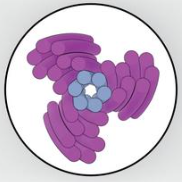

Scientists at the U.S. Department of Energy’s (DOE) Brookhaven National Laboratory, Columbia University, and Stony Brook University have developed a radical new method for producing a wide variety of designed metallic and semiconductor 3D nanostructures. The method uses a “hacked” form of DNA that instructs molecules to organize themselves into targeted 3D patterns.
The new method could produce robust nanostructures from multiple material classes. The study was recently published in Science Advances.
“We have been using DNA to program nanoscale materials for more than a decade,” said corresponding author Oleg Gang, a professor of chemical engineering and of applied physics and materials science at Columbia Engineering and leader of the Soft and Bio Nanomaterials Group at the Center for Functional Nanomaterials (CFN), a DOE Office of Science user facility at Brookhaven Lab.
“Now, by building on previous achievements, we have developed a method for converting these DNA-based structures into many types of functional inorganic 3D nano-architectures, and this opens tremendous opportunities for 3D nanoscale manufacturing.”
Next level of self-assembly: microelectronics and semiconductor devices
CFN is a leader in researching self-assembly, the process by which molecules spontaneously organize themselves. In particular, scientists at CFN are experts at DNA-directed assembly. Researchers program strands of DNA to “direct” the self-assembly process towards molecular arrangements that give rise to beneficial properties, such as electrical conductivity, photosensitivity, and magnetism. Then, those structures can be scaled up to functional materials.
To date, CFN has used DNA-directed assembly to produce switchable thin films, 3D nanosuperconductors, and more.
3D metallic nanostructures
“We have demonstrated various types of structures we can organize using DNA-directed assembly. But, to take this research to the next level, we can’t only rely on DNA,” Gang said. “We needed to expand upon our method to make more robust structures with more specific functionality for advanced technologies like microelectronics and semiconductor devices.”
Recently, Gang and colleagues were able to grow silica, an oxidized form of silicon, onto a DNA lattice. The addition of silica created a much more robust structure, but the procedure was not widely applicable to different materials. The team still needed further research to develop a method that could produce metallic and semiconductor materials in an efficient way.
So to build out a more universal method for producing 3D nanostructures, researchers in CFN’s Soft and Bio Nanomaterials Group collaborated with the Center’s Electronic Nanomaterials Group.
Scientists in this group pioneered a novel material synthesis technique called vapor-phase infiltration. This technique bonds a precursor chemical, in vapor form, to a nanoscale lattice, penetrating beyond the surface and deep into the material’s structure. Conducting this technique on the silica structures Gang’s team had previously built, using precursors with metallic elements, enabled the researchers to produce 3D metallic structures.
The team also experimented with liquid-phase infiltration, a technique that forms chemical bonds on a material’s surface, except with a liquid precursor. In this case, the team bonded different metal salts to silica, forming a variety of metallic structures. For example, they were able to combine platinum, aluminum, and zinc on top of one nanostructure.
The team was able to produce 3D nanostructures containing different combinations of zinc, aluminum, copper, molybdenum, tungsten, indium, tin, and platinum. This is the first demonstration of its kind for creating highly structured 3D nanomaterials.
There are several properties needed to make useful materials for technologies like semiconductor devices. For this study, the researchers imparted electrical conductivity and photoactivity on the 3D nanostructures.
Making world-leading research accessible; a liquid-handling robot
CFN will now work to apply the method to more complex research and offer it to visiting scientists. As a user facility, CFN makes its capabilities and expertise available to “users” across the country and the world.
The ecosystem of CFN’s expertise and facilities that benefited this research is also a benefit to users, and CFN is constantly expanding its offerings and making them more accessible. For example, scientists are looking to implement the new research method into one of the Center’s newest tools, a liquid-handling robot.
CFN also studies the mechanical properties of nanomaterials, and the materials like the ones developed in this work hold great potential for enhancing mechanical performance, as was recently shown by the group in another study, the researchers say.
“Overall, CFN’s new method for creating designed, robust, and functionally tunable 3D nanostructures has set the stage for breakthroughs in advanced manufacturing at small scales. Their work could enable diverse emerging technologies, and it will provide new opportunities for science initiatives and users at Brookhaven Lab.”
This study was supported by the DOE Office of Science.
Citation: Michelson, A., Subramanian, A., Kisslinger, K., Tiwale, N., Xiang, S., Shen, E., Kahn, J. S., Nykypanchuk, D., Yan, H., Nam, Y., & Gang, O. (2024). Three-dimensional nanoscale metal, metal oxide, and semiconductor frameworks through DNA-programmable assembly and templating. Science Advances. https://www.science.org/doi/10.1126/sciadv.adl0604 (open-access)
Let us know your thoughts! Sign up for a Mindplex account now, join our Telegram, or follow us on Twitter.


0 Comments
0 thoughts on “Scientists Hack DNA to Make Next-Gen Nanostructures”