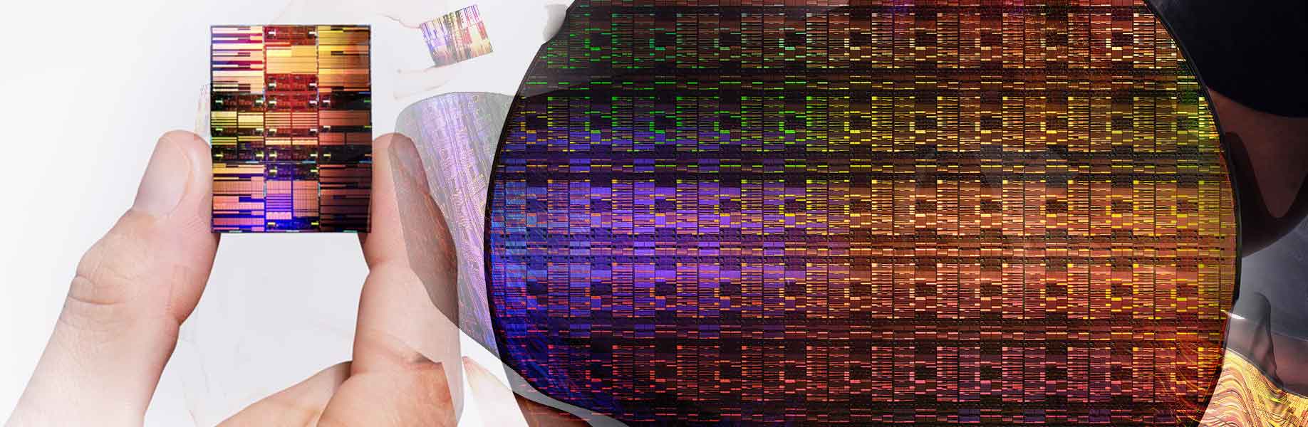

IBM has created the first chip technology that operates below the one-nanometer scale. This new process reaches 0.7 nanometers. The chip contains nearly 100 billion transistors on an area the size of a fingernail. This density is almost twice that of IBM’s earlier 2 nanometer chip from 2021.
The technology is expected to deliver up to 50 percent higher performance or 70 percent better energy efficiency than the previous 2 nanometer generation. These gains could support demanding uses such as artificial intelligence (AI) systems, cloud computing services, and other advanced electronic devices.
New three-dimensional transistor structure enables further scaling
The key advance is a new transistor design called nanostack. It builds on earlier nanosheet technology, in which transistors are made from extremely thin material layers. In the nanostack approach, these layers are stacked vertically in three dimensions rather than placed side by side. This arrangement allows more transistors to fit into the same space. Different material combinations can also be used in each layer, so each transistor can be optimized separately for speed or power efficiency.
Laboratory tests have shown that the structure can be manufactured and that it functions correctly in basic circuit elements. The design also improves memory efficiency, providing 40 percent better scaling in a common type of fast memory called SRAM. These results confirm that the technology supports actual computation.
The work continues IBM’s long record of semiconductor research. It was carried out at a facility in Albany, New York, where new high-resolution lithography equipment is being installed.
This "marks a landmark moment in computing, pushing technology beyond the nanometer era to the scale of atoms," said Jay Gambetta, Director of IBM Research," in a press release. "With our new nanostack architecture, we’re not just making smaller transistors, we’re reinventing how chips are built to deliver dramatically more power and energy efficiency."